Masimo Semiconductor operates a complete compound semiconductor device fabrication line focused on the fabrication of custom devices, as well as development, prototyping, pilot production and manufacturing. Capabilities of the custom and production wafer processing laboratory at Masimo Semiconductor range from prototype development to full production and include CAD design of photolithographic mask sets, development of custom device processes, and routine fabrication.
![]() |
Custom Power Converter |
![]() |
GaAs Space Solar Cell |
![]() |
Red LEDs |
![]() |
Space Applications |
![]() |
High Efficiency Space Cell |
![]() |
TPV Cells |
![]() |
Laser Diode |
![]() |
VCSEL Wafer close-up |
![]() |
VCSEL Wafer |
![]() |
Laser Power Converter |
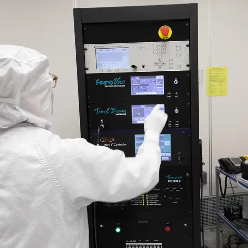
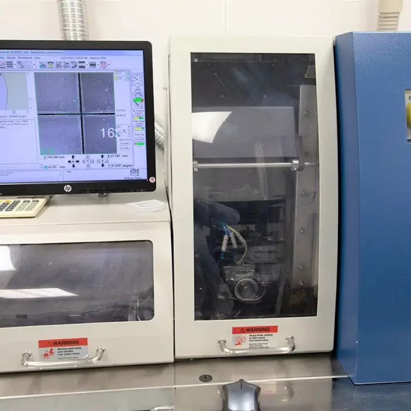
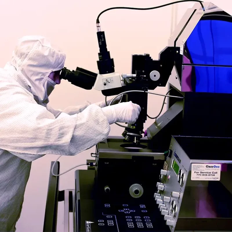
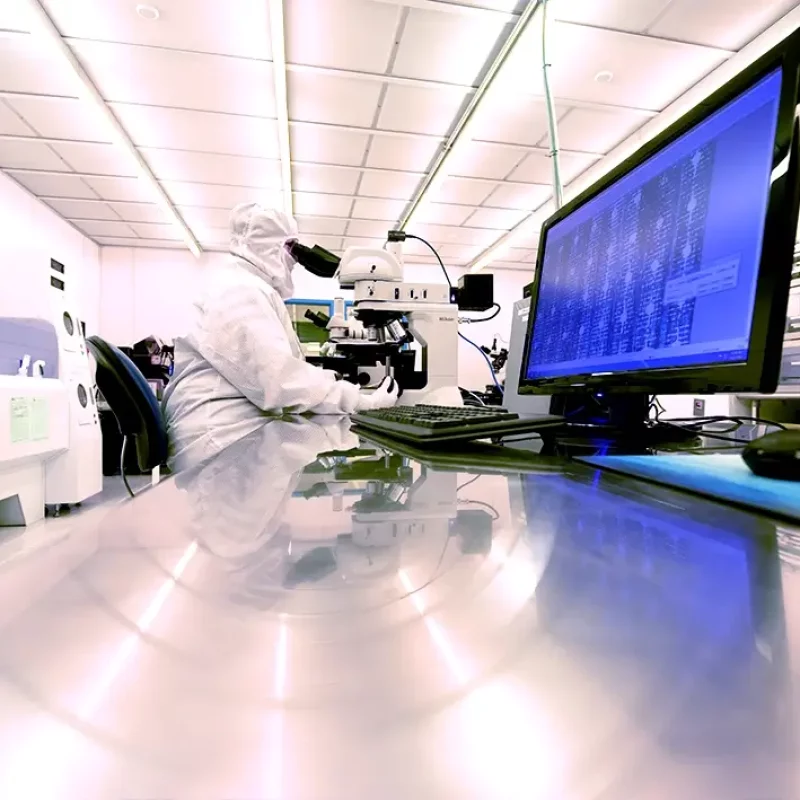
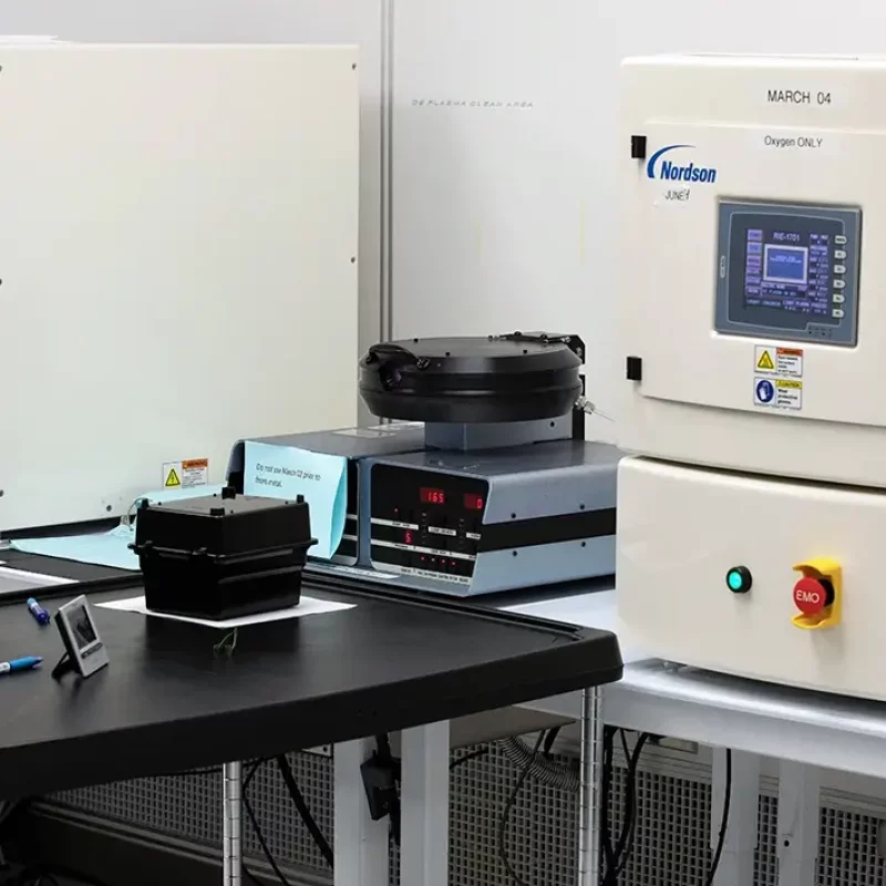
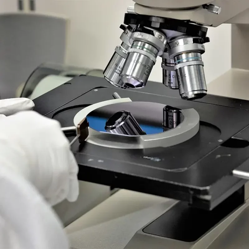
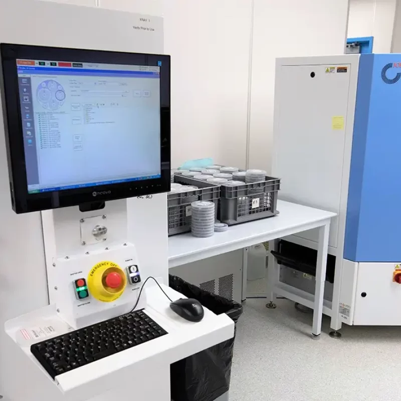
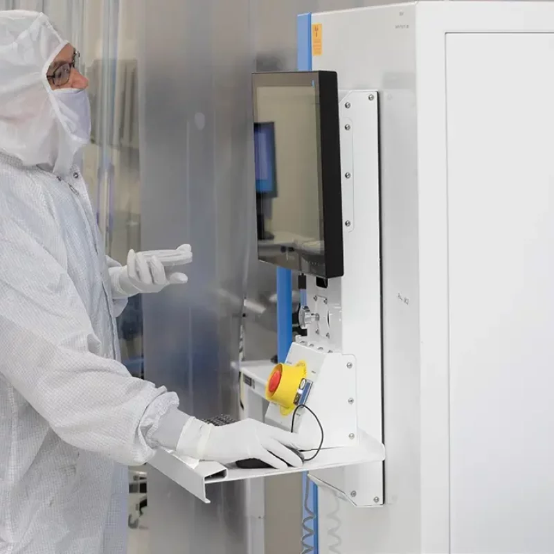
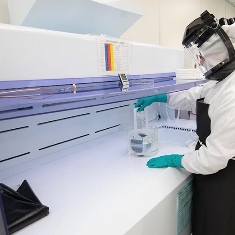
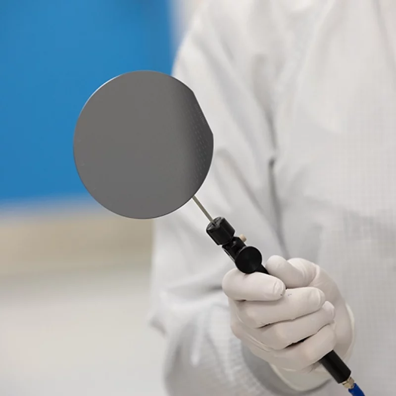
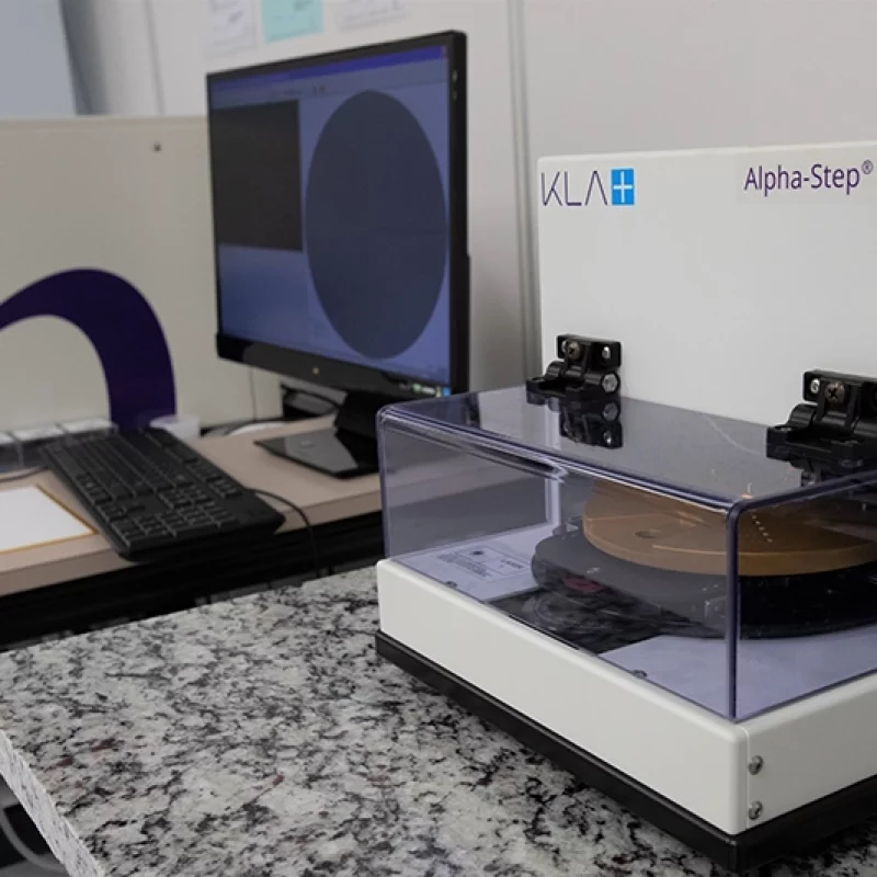
At Masimo Semiconductor, we take epitaxial wafers through the full wafer fabrication process flow. This includes GaAs, InP, Silicon, InAs, lithium niobate or lithium tantalate wafers up to 4 inches in size. These wafers can be grown at Masimo Semiconductor’s facility or supplied by customers. Customers can also supply photomasks, or we can provide the engineering expertise to develop a process flow and CAD layout used to develop a new set of masks or cross-sectional concept drawings. We specify the process steps or collaborate and agree on parameter conditions to meet the desired device feature and implement the process in our fabrication line. This saves development time for our customers and provides a source of proprietary devices without the expense of a dedicated internal fabrication line.
View a list of available brochures and request additional information. More»